A RISC-V design on real silicon
Dual Core RISC-V Tapeout with S3B and the Aussie Chip Collective
Lead silicon architect
Many computer engineers, myself included, got into the field to work on real chips. Unfortunately, there are currently no courses at UNSW that cover the whole RTL-to-GDS workflow, as most of the focus is on high level FPGA work. I'm one of 11 students who co-founded this project to give students the opportunity to learn the whole stack from year one. The current project, a dual-core RISC-V CPU on GF180, is largely based on the riskyC1 core and on track for submission on December 1. After that, we're planning to participate in a Jane Street competition and iterate on our design for next year.
The Idea
After riskyC1 passed every ISA test on my FPGA, I was looking for a new project to apply everything I had learned. Around this time, I joined our newly founded Computer Engineering Society as a subcom member, and it became clear that there were many other students interested in the same thing, so the tapeout project (we still don't have a better name for it) was born.
S3B and the Aussie Chip Collective agreed to fund a half-width slot on the uni's upcoming Tiny Tapeout, which would allow the team to demonstrate their ability to produce working silicon. Since the deadline was set as December 1, we decided to take my previous RISC-V IP and use it as the basis for a dual-core SoC, as this would allow us to learn & demonstrate a variety of capabilities. The design process so far is documented below.
Un-pipelining the core
After some initial discussions, it quickly became apparent that making a dual-core architecture work with the existing pipeline I built into riskyC1 would create a variety of data hazards. Since the primary goal for December was to get a working multicore chip, we decided to remove the pipeline entirely so we could focus on other things such as caches, the arbiter and the SRAM controller instead. In one afternoon session, I converted riskyC1 into "Bob", the multi-cycle core that would become the basis for our SoC.
Bob re-uses the same decoder, immediate generator and memory-access logic, but is driven by a small FSM: FETCH → EXEC → MEM → MEM_W → FETCH. ALU ops and branches take 2 cycles, stores 3, loads 4. The FSM simply absorbs the SRAM's latency as one extra state. Since we were constantly experimenting with different features under our area constraint, we decided to make some architectural decisions configurable using parameters:
- Default is RV32E (16 registers), with RV32I as a parameter. With 16 registers, x16–x31 read as zero and writes are dropped, so RV32I code fails loudly instead of silently aliasing.
- riskyC1's write-first register file bypass has to be off here. In a multicycle core it would close a combinational loop rs1 → ALU → rd. Fun one to find.
- The ALU got reworked for area: one 33-bit adder does ADD, SUB, SLT and SLTU, and one right-shifter does all three shifts (SLL just bit-reverses in and out, which is free wiring).
// One adder serves ADD, SUB, SLT and SLTU
assign do_sub = (ctrl == ALU_SUB) | (ctrl == ALU_SLT) | (ctrl == ALU_SLTU);
assign b_eff  = do_sub ? ~b : b;
assign sum33  = {1'b0, a} + {1'b0, b_eff} + {32'd0, do_sub};

// Unsigned a < b: no carry out of a - b.
assign ltu = ~sum33[32];
// Signed a < b: differing signs means a is smaller iff a is negative,
// otherwise the difference's sign bit decides.
assign lt = (a[31] ^ b[31]) ? a[31] : sum33[31];

// One right-shifter serves SLL, SRL and SRA
assign shamt     = b[4:0];
assign shift_src = (ctrl == ALU_SLL) ? rev32(a) : a;
assign sign_fill = (ctrl == ALU_SRA) ? shift_src[31] : 1'b0;
assign shift_ext = $signed({sign_fill, shift_src});
assign shifted   = 32'(shift_ext >>> shamt);
Optimized ALU: One adder, one shifter. Bit reversal is just wires, so SLL costs nothing extra.
Sharing one memory between two cores
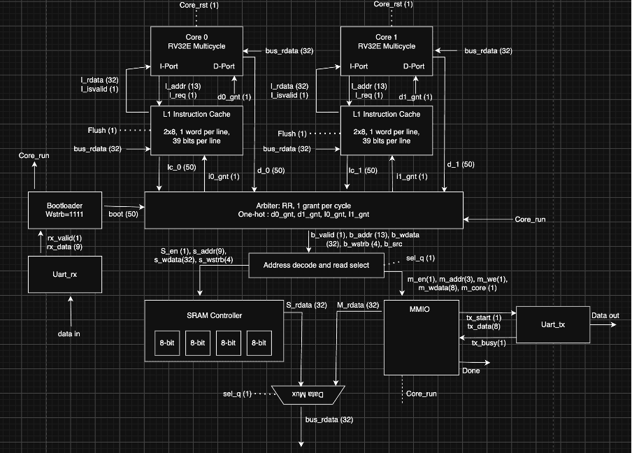
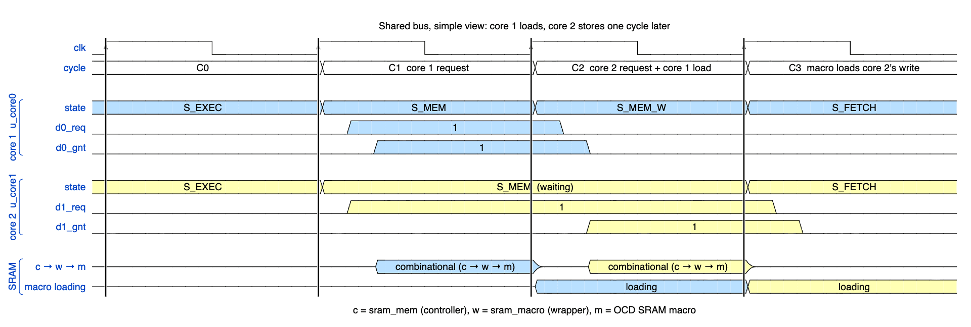
Since we decided to use SRAM macros for our memory, it might seem counterintuitive why we added an instruction cache. The issue is that our memory only allows for one access per cycle, so one core was consistently starved for data in our preliminary testing. By adding one instruction cache per core, we significantly improved performance even though accessing the cache takes the same time as the memory (1 cycle). The diagram below shows our v2 architecture, with five requesters on a shared bus and the arbiter granting one requester per cycle following a standard round-robin protocol. While a program is loading over UART, only the bootloader gets through.
We later decided to add a dcache as well, not so much to improve performance (it actually makes it worse in some cases), but so we could experiment with cache coherence and TAS/TTAS in the future. In the most recent version, we also pipelined the bus so access can be granted while the previous one's read data is still coming back, which is what keeps two cores from halving each other's throughput.
drive the bus arbiter yourself
One grant per cycle, decided combinationally. The pointer says who gets checked first and then moves to whoever is after the winner, so nobody starves. Keep clocking with three requesters on and watch it rotate.
- press clock ↑
An illustration of the arbiter logic. Coming from my single core, I found this illustration very useful to understand what's going on.
Memory, caches and coherence
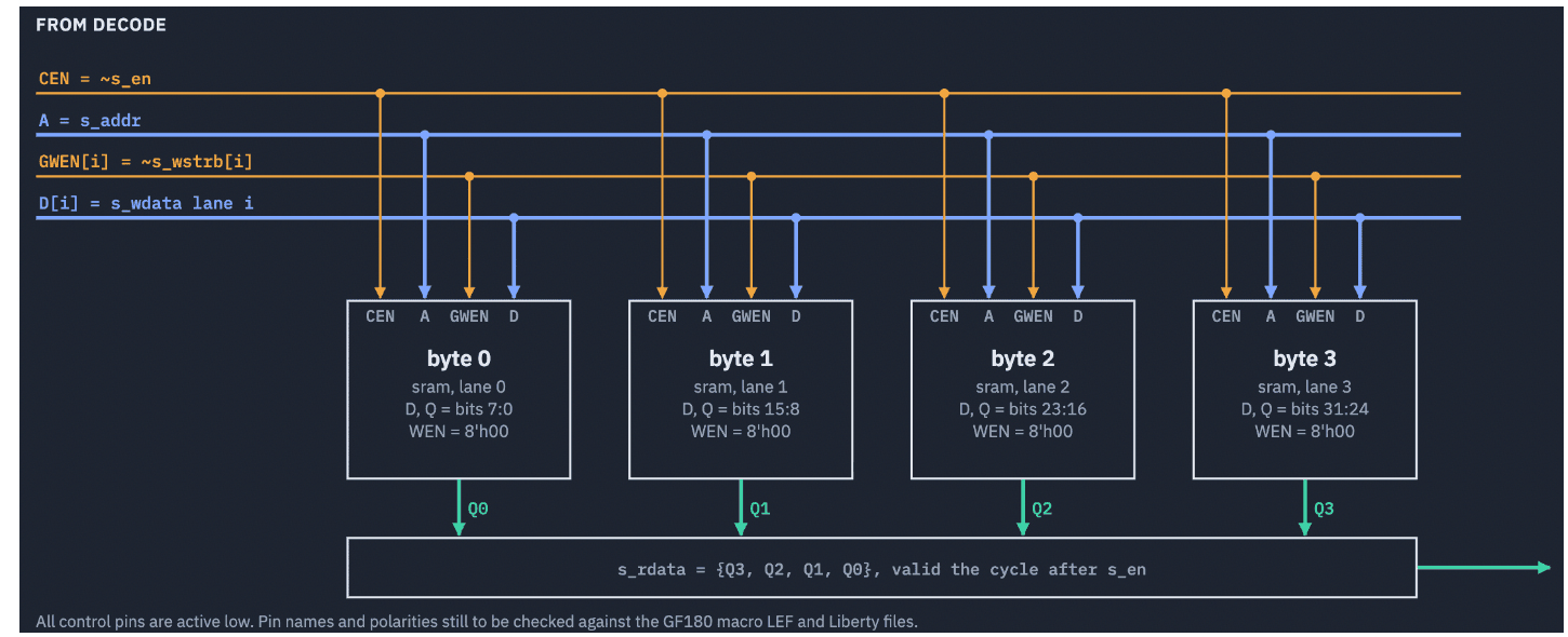
Since our RISC-V instructions are 32-bit wide, fitting four 8-bit GF180 SRAM macros side by side was essential for getting decent throughput. Every lane is enabled on every access and lane i only writes if its strobe is set, so sb, sh and sw all fall out naturally. The wrapper is the only file that knows the macros' pins are active-low.
Since the dcache was added relatively quickly and was not part of our original plan, we needed a way to disable it quickly, if testing showed that it would break our design. After talking to an AMD engineer, we changed the design so every cache can be switched off at load time with "chicken bits" in the bootloader header. If a cache turns out broken on the real chip, we can still demonstrate the project was a success.
Testing & Teamwork
Because of the enormous time pressure of the project, things started off relatively chaotic. I spent the first two weeks briefing everyone on RISC-V and the core I built, after which we would discuss potential architectures and features for hours. The area constraint meant that we could only include so many ideas, and since none of us had done a tapeout before, we wanted to make sure there would be enough time to verify everything.
After the initial architecture was settled, we decided to split the team into RTL, PD and verification teams. This proved essential as it would allow people to work in parallel, where new RTL features such as the dcache could be added while the older design was being validated. For testing, we set up two toolchains on purpose: Toolchain A (Verilator, Icarus, Yosys, cocotb, pinned with Nix) runs on every PR. Toolchain B (LibreLane physical design on the gf180mcuD PDK) runs at milestones against tagged RTL. The rough set up at the moment:
- The official riscv-tests plus an RV32E self-test pass at both 16 and 32 registers, both preloaded and through the real serial boot path.
- Multicore programs hammer the shared bits: two cores incrementing a counter under the MMIO test-and-set lock, 100 critical sections per core with mixed word/byte access, cache thrashing, back-to-back program reloads.
- The SRAM tests run against both a behavioural model and the vendor's actual macro models, which is what proves the active-low wiring: a wrong
CENorGWENfails every test. - Lint is
verilator -Wallwith explicit waivers. Any new warning fails CI.
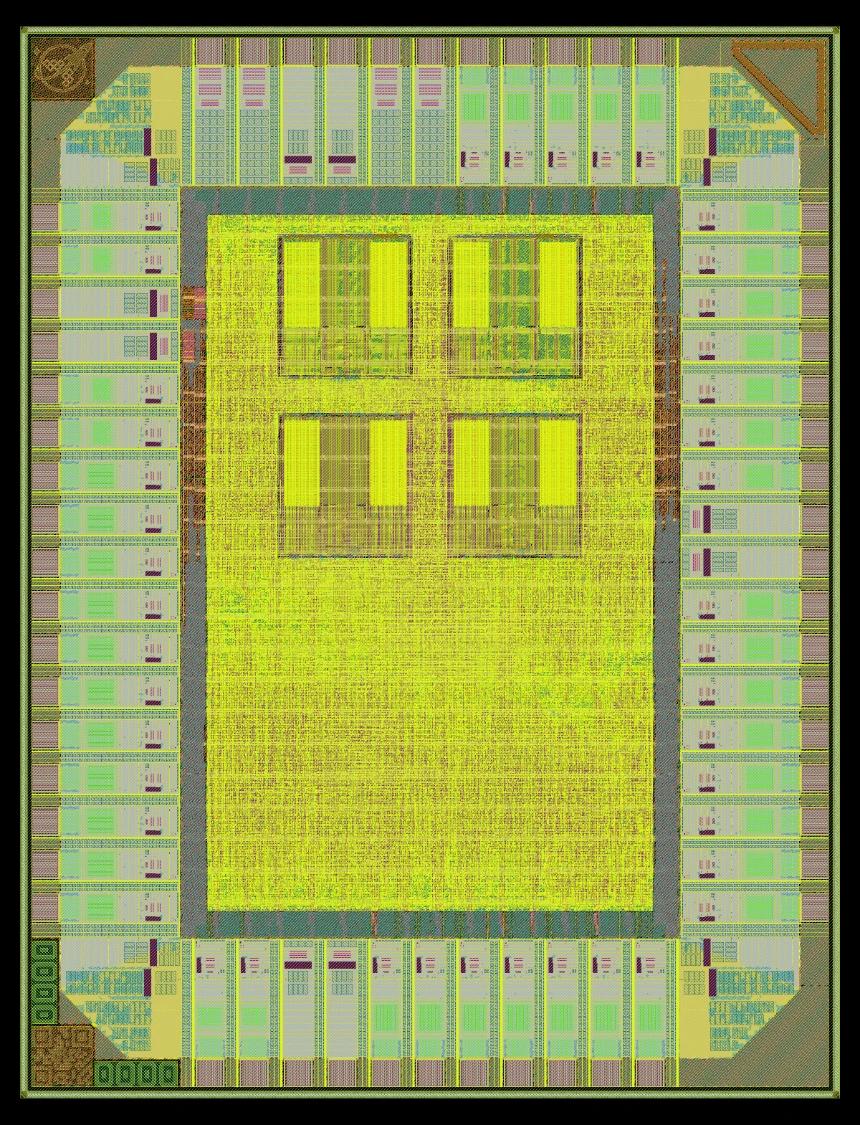
Next up: Final verification, then the Jane Street competition. We have many ideas on how to iterate on this design in the future, once we receive the necessary funding.