Analogue ECG front-end
Pulling a 1 mV heartbeat out of 50 Hz mains hum, using a bunch of op-amps and my first KiCAD design
Since most of my work is digital, I decided I wanted to experiment with a real analogue project, so when my professor suggested I could build an ECG circuit, I was hooked immediately. To effectively isolate an ECG signal on an oscilloscope, I built a five-stage biopotential amplifier: in-amp, high-pass, gain + low-pass, twin-T notch and right-leg drive. I derived the circuit, simulated it in LTSpice, abandoned the breadboard version after five hours of rail-slamming, then built it as a PCB that hit ×1104 gain, CMRR 561 and a clean, hum-free output. The bandwidth came out narrower than planned, but everything else ended up working in the end.
What the circuit has to do
An ECG signal at the skin is 0.5 to 2 mV. It's slow (60 bpm is 1 Hz), it sits on top of an electrode DC offset of up to ±300 mV, and it's buried under 50 Hz mains pickup that's much bigger than the signal itself.
So the job is: about ×1000 gain to get to a scope-friendly 1 V, a passband of roughly 0.5–40 Hz, and as much 50 Hz rejection as I can get. No single trick does all of that, so I split it into simple stages that each fix one problem and can be tested on their own.
Gain in the right order
After doing some initial research, I quickly realized that splitting the gain into two stages would likely yield better results than any single-stage approach. With a single ×1000 at the input, that ±300 mV electrode offset becomes ±300 V, instantly slamming the op-amp into the rails. Instead, the input amp only amplifies ×10, the high-pass strips the DC, followed by a larger ×101 gain stage. By interleaving the filtering between the stages, noise gets removed before it can eat headroom.
Getting rid of the mains hum turned out to be a team effort as well. The in-amp's common-mode rejection, the right-leg drive pushing the body's potential towards ground, the notch filter and the low-pass all contribute, but none of them is enough on its own. A plain low-pass, for example, only takes about 4 dB off at 50 Hz.
walk the signal chain
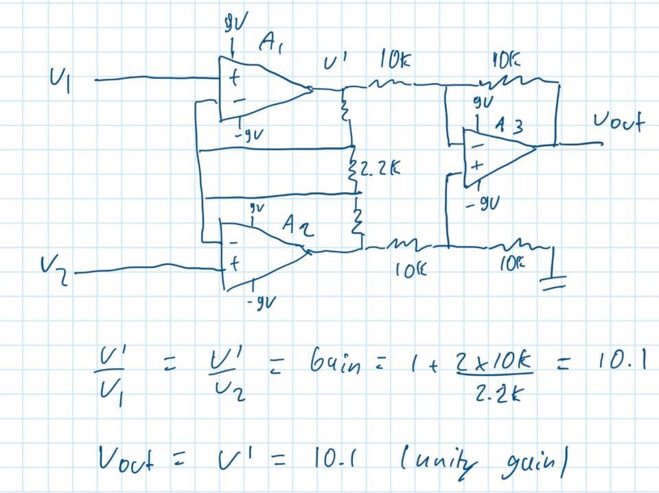
In-amp
Two buffers give the electrodes basically infinite input impedance, then a matched difference amp pulls out the differential signal. Only ×10 here on purpose: the skin–electrode junction can sit at ±300 mV DC, and ×1000 on that would slam straight into the rails.
R1 10 kΩ ×2 · Rg 2.2 kΩ · R2/R3 10 kΩ ×4 · TL074
Simulating first
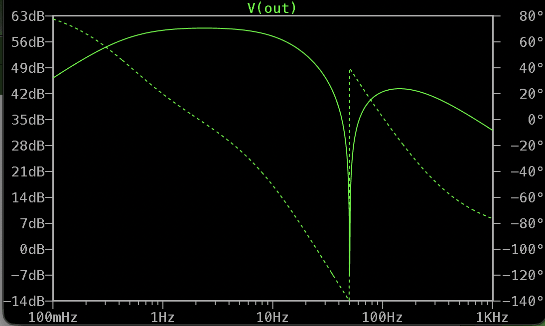
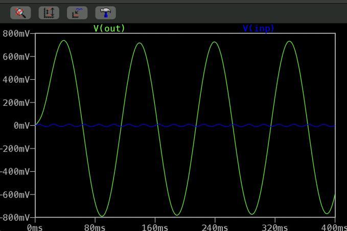
Before touching any hardware, I simulated the entire signal chain in LTSpice. I ended up writing it as a netlist instead of drawing it, since the schematic became unreadable very quickly, and modelled the op-amps as simple single-pole amplifiers. The AC sweep showed the band-pass shape I was hoping for, with roughly 60 dB of flat gain and a sharp null at 50 Hz. A transient run with a 1 mV test signal and 2 mV of 50 Hz hum on top also came out clean, so I was fairly confident going into the build.
From breadboard to PCB
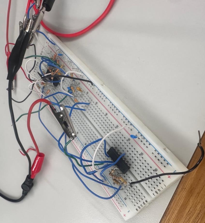
Unfortunately, reality didn't quite match the simulation. On the breadboard, even the first stage kept slamming into the rails, and after five hours of debugging I gave up on it. With 60 dB of gain and inputs in the microvolt range, contact resistance, the missing ground plane and stray coupling between jumper wires were simply bigger than the signal I was trying to measure.
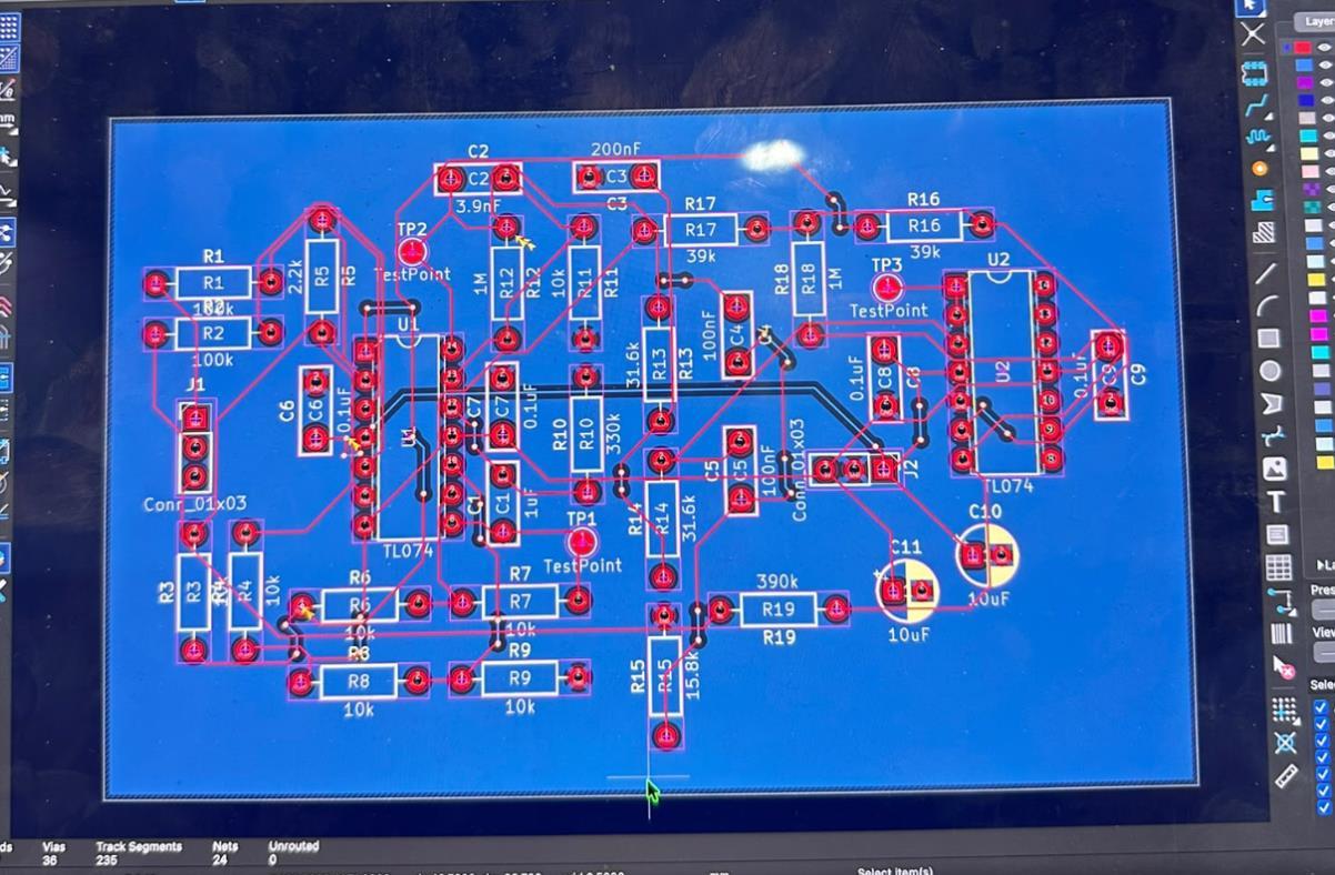
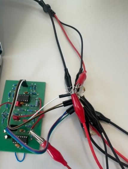
Since the simulation had given me confidence in the design, I simply imported the exact netlist into KiCAD and started working on a two-layer PCB. After the breadboard experience, I added three test points (after the in-amp, after the gain stage and at the final output) so I could check each stage on its own. In hindsight, those test points saved the project: the assembled board had three construction faults (a missing ground joint at R9, an open joint on U2 pin 1 and a transposed supply rail), and continuity testing stage by stage found all three.
What I measured
After finally fixing the continuity issues, I started by characterising each stage with a synthetic signal to eliminate any safety concerns. The results exceeded my expectations: the gain peaked at ×1104 (60.9 dB), and the CMRR came out at 561, almost exactly what 1% resistor matching predicts. That means the resistors are the limiting factor, not the TL074. The output noise floor was 28 mV, with no visible mains component at all.
Two things didn't go to plan, but both have clear explanations:
- The notch landed at 48 Hz instead of 50 Hz. I fitted a 33 kΩ resistor instead of the planned 31.8 kΩ, and 1/(2π · 33k · 100n) = 48.2 Hz, within 0.4% of what I measured. The trimmer in the design would fix this.
- The passband came out at 0.93–14.6 Hz instead of 0.5–40 Hz. This one comes from the passive twin-T. Its Q is only 0.25, so its attenuation starts well below 50 Hz and dominates the roll-off from about 20 Hz upwards, long before the 41 Hz low-pass kicks in. It's a design oversight in how the stages interact, not a build fault.
You can explore the second issue in the plot below. If you turn off the notch, the upper band edge jumps out. Raising the notch Q, which is what bootstrapping the twin-T from a buffer would do, brings most of the band back.
model vs bench, and the fix
- model −3 dB band
- 0.45–11.6 Hz
- measured band
- 0.93–14.6 Hz
- notch null
- 48.2 Hz
The amber dots are my bench measurements, and the green curve is a simple analytic model of the five stages based on the component values (not a fit, just the maths). The measured in-amp gain came in slightly high (22.4 dB vs 20 dB), which is why the model sits a little below the measurements.
| Test | Target | Measured | Verdict |
|---|---|---|---|
| Total gain | ×1000 | ×1104 peak | met |
| CMRR | > 500 | 561 | met |
| Notch depth | deep at 50 Hz | 37.4 dB @ 48 Hz | met |
| Noise floor | low | 28 mV, no hum | met |
| Passband | 0.5–40 Hz | 0.93–14.6 Hz | partly |
| Live ECG | PQRST | ran out of time | not tried |
Biggest lesson: theory and reality tend to diverge when working with analogue signals. While the initial design was done after about 5 hours, building and debugging took another 40. Also, high-gain analogue circuits don't belong on a breadboard.